
Seeing an RF design finally come together on the PCB is always a good moment.
But it is still only one step.
The first unit must be assembled, powered up and measured. That is when the small changes that only become obvious with real hardware on the bench begin to emerge.
From layout to physical hardware
The PCB layout brings the RF path, power distribution, control circuitry and mechanical interfaces into one design.
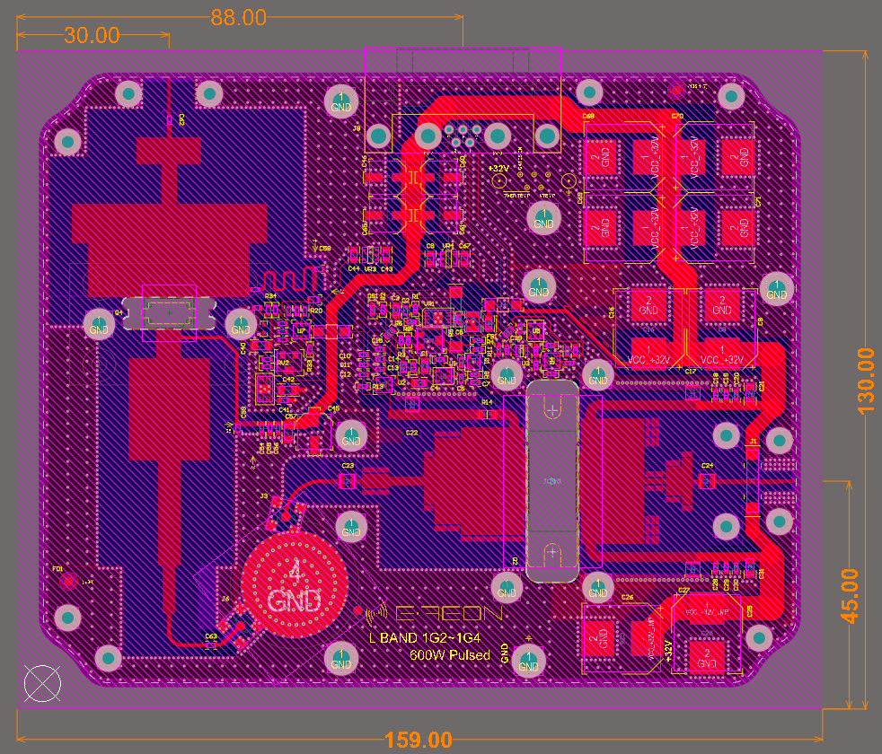
PCB layout for the 1.2-1.4 GHz, 600 W pulsed L-band amplifier.
The mechanical model is another part of the same engineering process. It allows the PCB, enclosure, connectors and internal components to be reviewed as one assembly before the complete hardware is built.
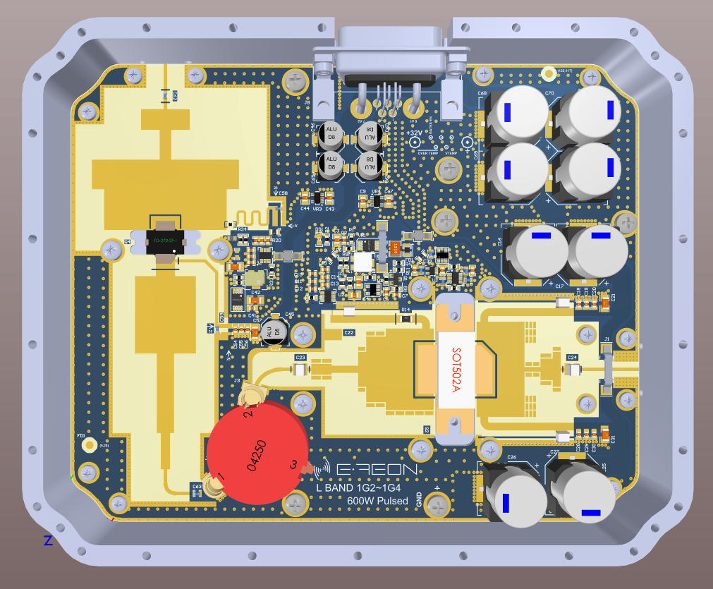
CAD representation of the amplifier PCB and enclosure assembly.
The first assembled unit
Once the first unit is on the bench, design decisions can be checked against the physical assembly and measured RF performance.
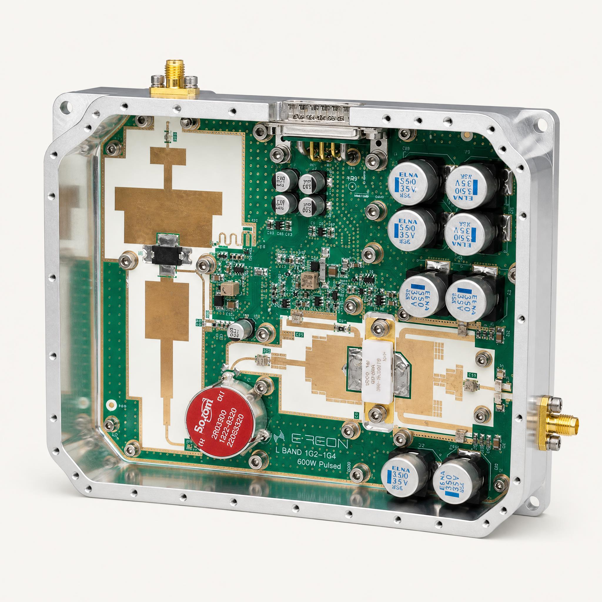
An assembled amplifier module before the enclosure is closed.
A successful first unit shows that the design works. Building more units starts to show whether the design can be assembled repeatedly while maintaining the intended mechanical and electrical interfaces.
From one working unit to repeatable hardware
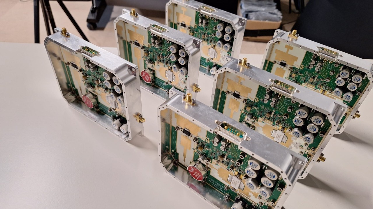
The finished modules are the visible result. Much of the engineering between the PCB layout, first assembly, measurement and subsequent builds is no longer visible once the covers are installed.
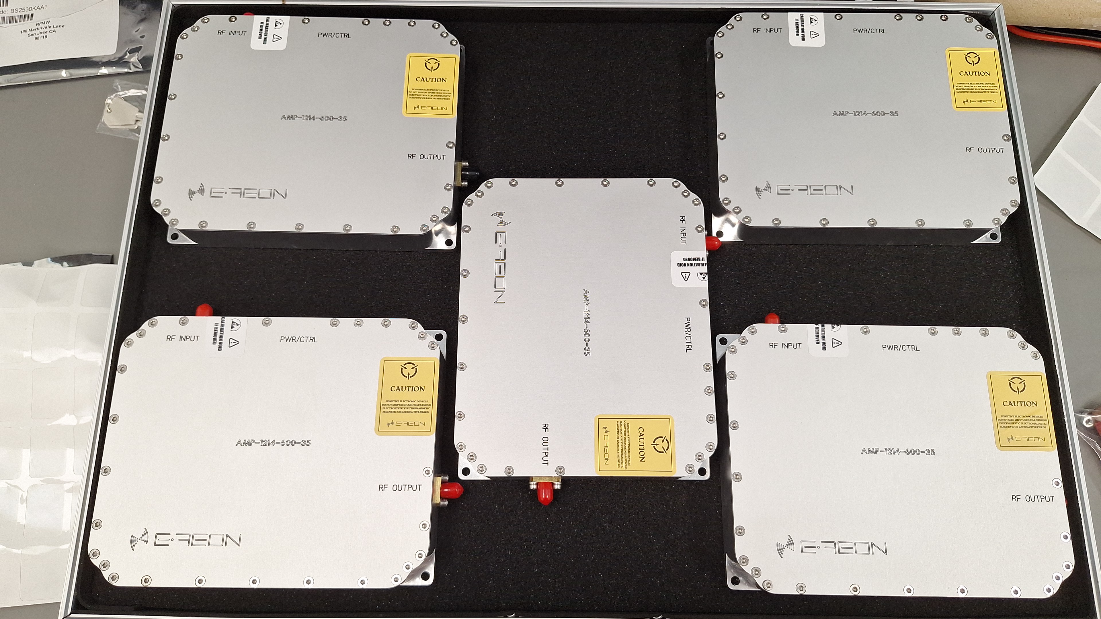
Finished amplifier units prepared after assembly and verification.
One good unit tells us that the design works. Several good units begin to show that we have hardware that can actually be built.
The PCB is only the beginning.